Decoder
A decoder is used to convert from an N-bit binary code to one of at most 2N possible outputs. The decoder is a common example of a combinational logic circuit.
Example
The following truth table shows a 3 to 8 decoder, a.k.a. an octal decoder.
The three input variables A2, A1, and A0 form the binary code,
and the variables X0 to X7 are the eight output variables (23=8).
As can be seen, for any given input only one output variable has the value 1 and all others are 0.
Note that some decoders have outputs that are the dual of this example, i.e. only one output variable has the value 0
and all others are 1.
A2 |
A1 |
A0 |
X0 |
X1 |
X2 |
X3 |
X4 |
X5 |
X6 |
X7 |
|---|---|---|---|---|---|---|---|---|---|---|
0 | 0 | 0 |
1 | 0 | 0 | 0 |
0 | 0 | 0 | 0 |
0 | 0 | 1 |
0 | 1 | 0 | 0 |
0 | 0 | 0 | 0 |
0 | 1 | 0 |
0 | 0 | 1 | 0 |
0 | 0 | 0 | 0 |
0 | 1 | 1 |
0 | 0 | 0 | 1 |
0 | 0 | 0 | 0 |
1 | 0 | 0 |
0 | 0 | 0 | 0 |
1 | 0 | 0 | 0 |
1 | 0 | 1 |
0 | 0 | 0 | 0 |
0 | 1 | 0 | 0 |
1 | 1 | 0 |
0 | 0 | 0 | 0 |
0 | 0 | 1 | 0 |
1 | 1 | 1 |
0 | 0 | 0 | 0 |
0 | 0 | 0 | 1 |
The decoder essentially translates a binary code input into a minterm.
Because of this, any Boolean expression in a sum of products form can be implemented
with a decoder and OR gates.
For example, if we look at the full adder's truth table, we see that the S output
is 1 for minterms m1, m2, m4 and m7.
Now using the octal decoder described above, we could connect A, B, and Cin to the decoder inputs
A2, A1, and A0 in that order, then take the decoder outputs X1, X2,
X4, and X7 as input to an OR gate, the output of which would be S.
Verilog
Below is the Verilog code for a structural model of an octal decoder with an enable input. An enable input is found on many decoders and can be used, for example, to link two 3 to 8 decoders to build a 4 to 16 decoder.
module octal_decoder(X0, X1, X2, X3, X4, X5, X6, X7, A2, A1, A0, E);
   output X0; // Minterm 0
   output X1; // Minterm 1
   output X2; // Minterm 2
   output X3; // Minterm 3
   output X4; // Minterm 4
   output X5; // Minterm 5
   output X6; // Minterm 6
   output X7; // Minterm 7

   input  A2;  // Input binary code most significant bit
   input  A1;  // Input binary code middle bit
   input  A0;  // Input binary code least significant bit

   input  E;   // Enable signal

   wire   A2n; // A2 negated
   wire   A1n; // A1 negated
   wire   A0n; // A0 negated

   not(A2n, A2);
   not(A1n, A1);
   not(A0n, A0);

   and(X0, A2n, A1n, A0n, E);  // Minterm 0: 000
   and(X1, A2n, A1n, A0, E);   // Minterm 1: 001
   and(X2, A2n, A1, A0n, E);   // Minterm 2: 010
   and(X3, A2n, A1, A0, E);    // Minterm 3: 011
   and(X4, A2, A1n, A0n, E);   // Minterm 4: 100
   and(X5, A2, A1n, A0, E);    // Minterm 5: 101
   and(X6, A2, A1, A0n, E);    // Minterm 6: 110
   and(X7, A2, A1, A0, E);     // Minterm 7: 111
endmodule
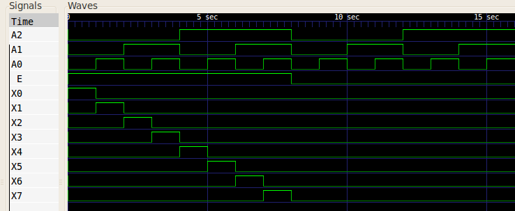
A simulation with test inputs gave the following wave form:
References
Kleitz, W. Digital Microprocessor Fundamentals. 3rd Edition. Prentice Hall, 2000.
Mano, M. Morris, and Kime, Charles R. Logic and Computer Design Fundamentals. 2nd Edition. Prentice Hall, 2000.