SR Flip-Flop (master-slave)
A SR flip-flop is used in clocked sequential logic circuits to store one bit of data.
It is similar in function to a gated SR latch but with one major difference: where the gated latch can have
its data set and reset many times whilst the gate input is 1, the flip-flop can only have the data set or reset once during a
clock cycle.
The latch is said to be transparent as the outputs see the inputs when the gate input is 1.
This transparency can be a problem in sequential logic circuits driven by a clock input if we want
at most one circuit state transition per clock period.
To see why, imagine a latch connected to another circuit which in turn is connected to the latch's set or reset inputs,
and let the clock signal be connected to the latch's gate input.
During each clock cycle, the changes in the latch's inputs are fed directly to the rest of the circuit which is fed back directly to the
latch's inputs.
This has the potential to give several state changes within a single clock period.
The basic idea of the flip-flop is the removal of this transparency which stops the latch's inputs feeding back through the circuit in a
single clock cycle.
This would give us a sequential circuit which can make at most one state change per clock period.
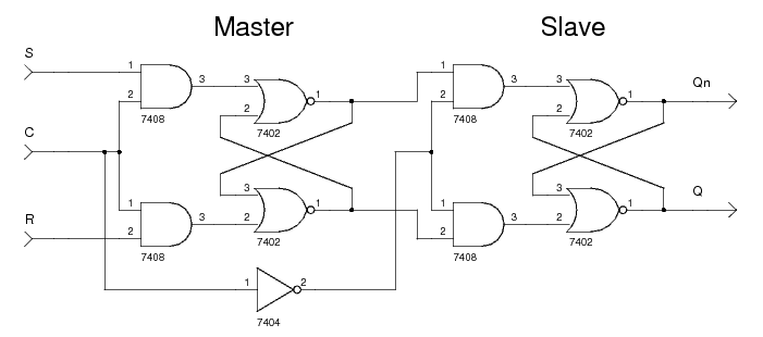
The type of SR flip-flop described here is a master-slave SR flip-flop.
It is built from two gated SR latches: one a master, and the other a slave.
The master takes the flip-flops inputs: S (set), R (reset), and C (clock).
The clock input is fed to the latch's gate input.
The slave takes the master's outputs as inputs (Q to S and Qn to R),
and the complement of the flip-flop's clock input.
The slave's outputs are the flip-flop's outputs.
This difference in clock inputs between the two latches disconnects them and
eliminates the transparency between the flip-flop's inputs and outputs.
The schematic below shows a master-slave SR flip-flop.
The two inputs S and R are used to set and reset the data respectively.
The clock input C is used to control both the master and slave latches making sure only one of the latches can set its data at
any given time.
When C has the value 1, the master latch can set its data and the slave latch cannot.
When C has the value 0, the slave can set its data and the master cannot.
From this description we see that the flip-flop is level-triggered.
The outputs Q and Qn are the flip-flop's stored data and the complement of the flip-flop's stored data respectively.
Example
The following function table shows the operation of a SR master-slave flip-flop. The column header Q(t+1) means
"the value of Q at the start of the next clock period", similarly for Qn(t+1).
S |
R |
Q(t+1) |
Qn(t+1) |
Meaning |
|---|---|---|---|---|
0 | 0 | Q | Qn | Hold |
0 | 1 | 0 | 1 | Reset |
1 | 0 | 1 | 0 | Set |
1 | 1 | ? | ? | Undefined |
Verilog
Below is the Verilog code for a structural model of a SR master-slave flip-flop. The code for the gated SR latch is also shown for completeness.
module sr_flip_flop_master_slave(Q, Qn, C, S, R);
   output Q;
   output Qn;
   input  C;
   input  S;
   input  R;

   wire   MQ;  // The master's Q output.
   wire   MQn; // The master's Qn output.
   wire   Cn;  // The clock input to the slave shall be the complement of the master's.

   not(Cn, C);
   sr_latch_gated master(MQ, MQn, C, S, R);
   sr_latch_gated slave(Q, Qn, Cn, MQ, MQn);
endmodule // sr_flip_flop_master_slave

module sr_latch_gated(Q, Qn, G, S, R);
   output Q;
   output Qn;
   input  G;
   input  S;
   input  R;

   wire   S1;
   wire   R1;

   and(S1, G, S);
   and(R1, G, R);
   nor(Qn, S1, Q);
   nor(Q, R1, Qn);
endmodule // sr_latch_gated
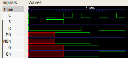
A simulation with test inputs gave the following wave form:
References
Kleitz, W. Digital Microprocessor Fundamentals. 3rd Edition. Prentice Hall, 2000.
Mano, M. Morris, and Kime, Charles R. Logic and Computer Design Fundamentals. 2nd Edition. Prentice Hall, 2000.