D Flip-Flop (edge-triggered)
A D flip-flop is used in clocked sequential logic circuits to store one bit of data.
The D flip-flop described here is positive edge-triggered which means that the input which is stored is that input which is
seen when the input clock transitions from 0 to 1.
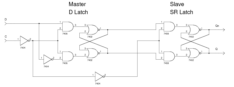
This flip-flop is built from two gated latches: one a master D latch, and the other a slave
SR latch.
The master takes the flip-flops inputs: D (data) and C (clock).
The clock input is inverted and fed to the D latch's gate input.
The slave takes the master's outputs as inputs (Q to S and Qn to R),
and the complement of the master's clock input.
The slave's outputs are the flip-flop's outputs.
This difference in clock inputs between the two latches disconnects them and
eliminates the transparency between the flip-flop's inputs and outputs.
The schematic below shows a positive edge-triggered D flip-flop.
The input D is used to set and reset the flip-flop's data.
The clock input C is used to control both the master and slave latches making sure only one of the latches can set its data at
any given time.
When C has the value 1, the slave can set its data and the master cannot.
When C has the value 0, the master can set its data and the slave cannot.
When C transitions from 0 to 1 the master has its outputs set which reflect the flip-flop's inputs when the
transition occurred.
The outputs Q and Qn are the flip-flop's stored data and the complement of the flip-flop's stored data respectively.
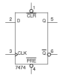
The schematic symbol for a 7474 edge-triggered D flip-flop is shown below. This chip has inputs to asynchronously clear and set the flip-flop's data.
Example
The following function table shows the operation of a D flip-flop. The column header Q(t+1) means
"the value of Q at the start of the next clock period", similarly for Qn(t+1).
D |
Q(t+1) |
Qn(t+1) |
Meaning |
|---|---|---|---|
0 | 0 | 1 | Reset |
1 | 1 | 0 | Set |
Verilog
Below is the Verilog code for a structural model of a positive edge-triggered D flip-flop. The code for the gated D and SR latches is also shown for completeness.
module d_flip_flop_edge_triggered(Q, Qn, C, D);
   output Q;
   output Qn;
   input  C;
   input  D;

   wire   Cn;   // Control input to the D latch.
   wire   Cnn;  // Control input to the SR latch.
   wire   DQ;   // Output from the D latch, input to the gated SR latch.
   wire   DQn;  // Output from the D latch, input to the gated SR latch.

   not(Cn, C);
   not(Cnn, Cn);
   d_latch dl(DQ, DQn, Cn, D);
   sr_latch_gated sr(Q, Qn, Cnn, DQ, DQn);
endmodule // d_flip_flop_edge_triggered

module d_latch(Q, Qn, G, D);
   output Q;
   output Qn;
   input  G;
   input  D;

   wire   Dn;
   wire   D1;
   wire   Dn1;

   not(Dn, D);
   and(D1, G, D);
   and(Dn1, G, Dn);
   nor(Qn, D1, Q);
   nor(Q, Dn1, Qn);
endmodule // d_latch

module sr_latch_gated(Q, Qn, G, S, R);
   output Q;
   output Qn;
   input  G;
   input  S;
   input  R;

   wire   S1;
   wire   R1;

   and(S1, G, S);
   and(R1, G, R);
   nor(Qn, S1, Q);
   nor(Q, R1, Qn);
endmodule // sr_latch_gated
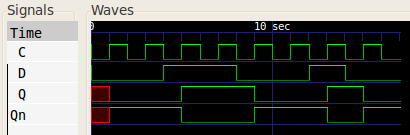
A simulation with test inputs gave the following wave form:
References
Kleitz, W. Digital Microprocessor Fundamentals. 3rd Edition. Prentice Hall, 2000.
Mano, M. Morris, and Kime, Charles R. Logic and Computer Design Fundamentals. 2nd Edition. Prentice Hall, 2000.