Datapath
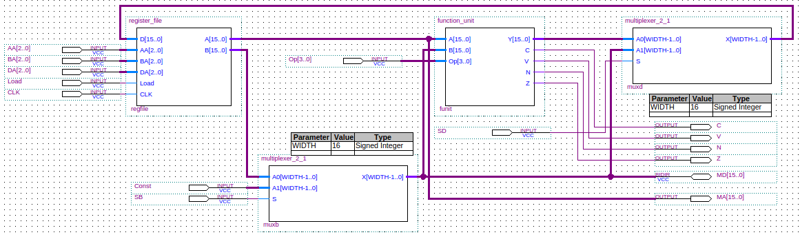
The datapath is the part of a digital system that performs the data processing. A typical datapath comprises a register file and a function unit. Values can be read from the register file and sent to the function unit or memory (RAM). Results from the function unit or data from memory (RAM or ROM) can be loaded into a register in the register file.
Example
We can combine our function unit and
register file examples with two multiplexers
(muxb and muxd):
one (muxb) to allow us to select between a register's contents or a constant value as one of the function unit inputs,
and the other (muxd) to choose between the function unit's operation output and memory data bus contents as the input to the
register file.
We will use the datapath inputs SB and SD as selection inputs to our two multiplexers.
The interface to memory will be an output to the memory address bus, MA, and an input/output to the memory data bus, MD.
There will be an input called Const which will allow us to send a constant value to the ALU or memory.
The datapath will need inputs AA, BA, DA, Load, and CLK for the
register file.
The description of the register file explains their meaning in more detail.
An input called Op will be passed directly to the function unit to determine the operation to be performed.
The function unit status bit outputs C, V, N, and Z will also be output by the datapath.
The description of the function unit explains their meaning in more detail.
The schematic form of the datapath is:
Below is the Verilog code for the datapath. The code for the other structures (function unit, register file, and multiplexer) has been omitted. See the notes for these structures for the code — more information at the links given earlier.
module datapath(C, V, N, Z, MA, MD, Op, AA, BA, DA, Load, Const, SB, SD, CLK);
   output C;            // Carry status bit.
   output V;            // oVerflow status bit.
   output N;            // Negative status bit.
   output Z;            // Zero status bit.
   output [15:0] MA;    // Memory address.
   inout [15:0]  MD;    // Memory data.
   input [3:0] 	 Op;    // Operation code.
   input [2:0] 	 AA;    // Address of A reg.
   input [2:0] 	 BA;    // Address of B reg.
   input [2:0] 	 DA;    // Address of C reg.
   input 	 Load;  // Enable loading of D reg - active high.
   input [15:0]  Const; // Constant.
   input 	 SB;    // Muxb selector.
   input 	 SD;    // Muxd selector.
   input 	 CLK;   // Clock.

   wire [15:0] A;
   wire [15:0] B0;
   wire [15:0] B1;
   wire [15:0] D;
   wire [15:0] Y;

   assign MA = A;
   assign MD = (SD == 1'b0) ? B1 : 16'bz;

   register_file regfile(A, B0, D, AA, BA, DA, Load, CLK);
   function_unit funit(Y, C, V, N, Z, A, B1, Op);
   multiplexer_2_1 muxb(B1, B0, Const, SB);
   multiplexer_2_1 muxd(D, Y, MD, SD);
endmodule // datapath
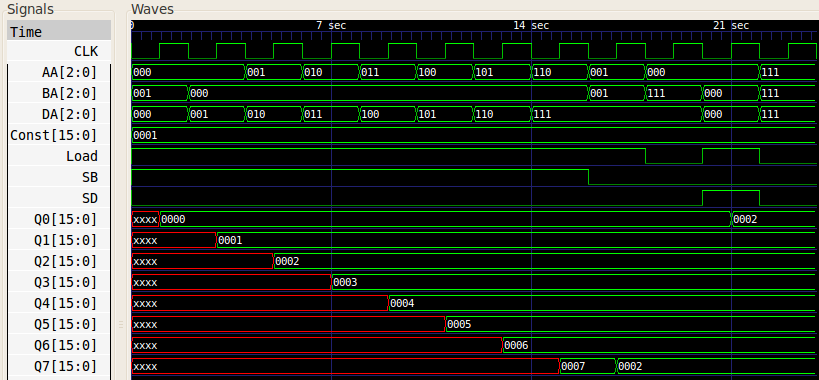
The datapath gave the waveform shown below when test inputs were given.
The test inputs involved first clearing register 0 (Q0), then for the rest of the registers 1, to 7,
(Q1, to Q7) we loaded the result of adding the contents of the previous register and the constant 1.
We then see an addition of register 1 with itself loaded into register 7.
Register 7 is then written to memory address 0, and then finally, the contents of memory address 0 are written into register 0.
References
Mano, M. Morris, and Kime, Charles R. Logic and Computer Design Fundamentals. 2nd Edition. Prentice Hall, 2000.