JK Flip-Flop (master-slave)
A JK flip-flop is used in clocked sequential logic circuits to store one bit of data. It is similar in function to a SR flip-flop.
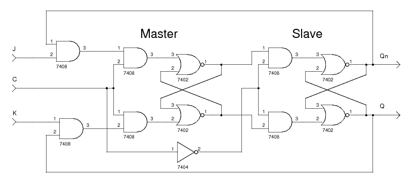
The schematic below shows a master-slave JK flip-flop.
As can be seen it is a simple modification of the master-slave SR flip-flop design — the outputs have been fed back and combined
with the inputs.
The two inputs J and K are used to set and reset the data respectively.
Together they can be used to toggle the data.
The clock input C is used to control both the master and slave latches making sure only one of the latches can set its data at
any given time.
When C has the value 1, the master latch can set its data and the slave latch cannot.
When C has the value 0, the slave can set its data and the master cannot.
From this description we see that the flip-flop is level-triggered.
The outputs Q and Qn are the flip-flop's stored data and the complement of the flip-flop's stored data respectively.
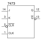
The schematic symbol for a 7473 level-triggered JK flip-flop is shown below. This chip has an input to asynchronously clear the flip-flop's data.
Example
The following function table shows the operation of a JK flip-flop. The column header Q(t+1) means
"the value of Q at the start of the next clock period", similarly for Qn(t+1).
J |
K |
Q(t+1) |
Qn(t+1) |
Meaning |
|---|---|---|---|---|
0 | 0 | Q | Qn | Hold |
0 | 1 | 0 | 1 | Reset |
1 | 0 | 1 | 0 | Set |
1 | 1 | Qn | Q | Toggle |
Verilog
Below is the Verilog code for a master-slave JK flip-flop. The code does not match the schematic exactly as an input was introduced to asynchronously reset the flip-flop. The code for the gated SR latch is also shown for completeness.
module jk_flip_flop_master_slave(Q, Qn, C, J, K, RESETn);
   output Q;
   output Qn;
   input  C;
   input  J;
   input  K;
   input  RESETn; // Active low reset signal.

   wire   MQ;  // The master's Q output.
   wire   MQn; // The master's Qn output.
   wire   Cn;  // The clock input to the slave shall be the complement of the master's.
   wire   J1;
   wire   K1;
   wire   J2;  // The actual input to the first SR latch (S).
   wire   K2;  // The actual input to the first SR latch (R).

   assign J2 = !RESETn ? 0 : J1;  // Upon reset force J2 = 0
   assign K2 = !RESETn ? 1 : K1;  // Upon reset force K2 = 1

   and(J1, J, Qn);
   and(K1, K, Q);
   not(Cn, C);
   sr_latch_gated master(MQ, MQn, C, J2, K2);
   sr_latch_gated slave(Q, Qn, Cn, MQ, MQn);
endmodule // jk_flip_flop_master_slave

module sr_latch_gated(Q, Qn, G, S, R);
   output Q;
   output Qn;
   input  G;
   input  S;
   input  R;

   wire   S1;
   wire   R1;

   and(S1, G, S);
   and(R1, G, R);
   nor(Qn, S1, Q);
   nor(Q, R1, Qn);
endmodule // sr_latch_gated
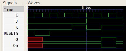
A simulation with test inputs gave the following wave form:
References
Kleitz, W. Digital Microprocessor Fundamentals. 3rd Edition. Prentice Hall, 2000.
Mano, M. Morris, and Kime, Charles R. Logic and Computer Design Fundamentals. 2nd Edition. Prentice Hall, 2000.