Register (Parallel Load)
A register is a collection of flip-flops.
Example
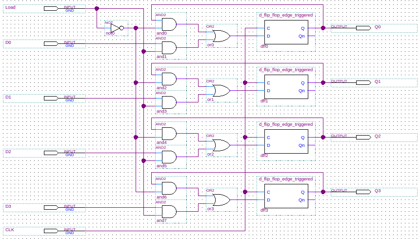
The example given here is a 4-bit parallel load register.
This register will be built around four edge triggered D flip-flops.
The register has four data input bits: D0, D1, D2, and D3.
In addition the register also has four data output bits: Q0, Q1, Q2, and Q3.
There is a Load input which, when at logic level 1, sets the four flip-flop data inputs to the register's four input bits.
When Load is at logic level 0, the four flip-flops have their outputs fed into their inputs.
This effectively disables loading from the four input bits.
In schematic form we have the following:
Verilog
Below is a Verilog structural model for the parallel load register. All code for the D flip-flops is given as well.
module register_parallel_load(Q0, Q1, Q2, Q3, D0, D1, D2, D3, Load, CLK);
   output Q0;    // Register output least significant bit.
   output Q1;
   output Q2;
   output Q3;    // Register output most significant bit.
   input  D0;    // Register input least significant bit.
   input  D1;
   input  D2;
   input  D3;    // Register input most significant bit.
   input  Load;
   input  CLK;

   wire   Loadn;
   wire   w1, w2, w3, w4, w5, w6, w7, w8, w9, w10, w11, w12; // Connecting wires.
   wire   Q0n, Q1n, Q2n, Q3n;   // Unused.

   not(Loadn, Load);

   and(w1, Q0, Loadn);
   and(w2, D0, Load);
   or(w3, w2, w1);

   and(w4, Q1, Loadn);
   and(w5, D1, Load);
   or(w6, w5, w4);

   and(w7, Q2, Loadn);
   and(w8, D2, Load);
   or(w9, w8, w7);

   and(w10, Q3, Loadn);
   and(w11, D3, Load);
   or(w12, w11, w10);

   d_flip_flop_edge_triggered dff0(Q0, Q0n, CLK, w3);
   d_flip_flop_edge_triggered dff1(Q1, Q1n, CLK, w6);
   d_flip_flop_edge_triggered dff2(Q2, Q2n, CLK, w9);
   d_flip_flop_edge_triggered dff3(Q3, Q3n, CLK, w12);
endmodule // register_parallel_load

module d_flip_flop_edge_triggered(Q, Qn, C, D);
   output Q;
   output Qn;
   input  C;
   input  D;

   wire   Cn;   // Control input to the D latch.
   wire   Cnn;  // Control input to the SR latch.
   wire   DQ;   // Output from the D latch, inputs to the gated SR latch.
   wire   DQn;  // Output from the D latch, inputs to the gated SR latch.

   not(Cn, C);
   not(Cnn, Cn);
   d_latch dl(DQ, DQn, Cn, D);
   sr_latch_gated sr(Q, Qn, Cnn, DQ, DQn);
endmodule // d_flip_flop_edge_triggered

module d_latch(Q, Qn, G, D);
   output Q;
   output Qn;
   input  G;
   input  D;

   wire   Dn;
   wire   D1;
   wire   Dn1;

   not(Dn, D);
   and(D1, G, D);
   and(Dn1, G, Dn);
   nor(Qn, D1, Q);
   nor(Q, Dn1, Qn);
endmodule // d_latch

module sr_latch_gated(Q, Qn, G, S, R);
   output Q;
   output Qn;
   input  G;
   input  S;
   input  R;

   wire   S1;
   wire   R1;

   and(S1, G, S);
   and(R1, G, R);
   nor(Qn, S1, Q);
   nor(Q, R1, Qn);
endmodule // sr_latch_gated
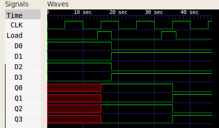
Below you can see the waveforms produced when the register was loaded twice.
References
Mano, M. Morris, and Kime, Charles R. Logic and Computer Design Fundamentals. 2nd Edition. Prentice Hall, 2000.