Shift Register (Bidirectional)
A shift register is a type of register which can have its contents shifted to the left or right.
Example
The example given here is a 4-bit parallel load bidirectional shift register.
This register will be built around four multiplexer and
edge triggered D flip-flop pairs.
The register has four data input bits: D0, D1, D2, and D3.
In addition the register also has four data output bits: Q0, Q1, Q2, and Q3.
There is a 2-bit selection input: S1, SO.
The function performed depends upon the selection input as described in the following table:
S1 |
S0 |
Function |
|---|---|---|
0
| 0
| Shift left |
0
| 1
| Shift right |
1
| 0
| Do nothing |
1
| 1
| Load register |
A shift to the right moves the value of bit N to bit (N-1) and he value of bit 0 is moved to bit 4. A shift to the left moves the value of bit N to bit (N+1) and the value of bit 4 is moved to bit 0.
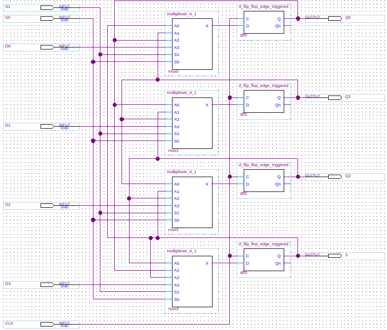
The design involves a positive edge triggered D flip-flop to hold the bit data and a multiplexer with four inputs (bit to the right, bit to the left, current output bit, register input bit) which are selected to set the flip-flops data on the next positive clock edge. In schematic form we have the following:
Verilog
Below is a Verilog model for the 4-bit bidirectional shift register. All code for the multiplexer and D flip-flops is given as well.
module shift_register_bidirectional(Q3, Q2, Q1, Q0, D3, D2, D1, D0, S1, S0, CLK);
   output Q3;  // Register output most significant bit.
   output Q2;
   output Q1;
   output Q0;  // Register output least significant bit.
   input  D3;  // Register input most significant bit.
   input  D2;
   input  D1;
   input  D0;  // Register input least significant bit.
   input  S1;  // MUX selector most significant bit.
   input  S0;  // MUX selector least significant bit.
   input  CLK;

   wire   Q3n, Q2n, Q1n, Q0n;
   wire   X3, X2, X1, X0;

   multiplexer_4_1 #(1) mux0(X0, Q3, Q1, Q0, D0, S1, S0);
   d_flip_flop_edge_triggered dff0(Q0, Q0n, CLK, X0);
   multiplexer_4_1 #(1) mux1(X1, Q0, Q2, Q1, D1, S1, S0);
   d_flip_flop_edge_triggered dff1(Q1, Q1n, CLK, X1);
   multiplexer_4_1 #(1) mux2(X2, Q1, Q3, Q2, D2, S1, S0);
   d_flip_flop_edge_triggered dff2(Q2, Q2n, CLK, X2);
   multiplexer_4_1 #(1) mux3(X3, Q2, Q0, Q3, D3, S1, S0);
   d_flip_flop_edge_triggered dff3(Q3, Q3n, CLK, X3);
endmodule // shift_register_bidirectional

module multiplexer_4_1(X, A0, A1, A2, A3, S1, S0);
   parameter WIDTH=16;     // How many bits wide are the lines

   output [WIDTH-1:0] X;   // The output line

   input [WIDTH-1:0]  A3;  // Input line with id 2'b11
   input [WIDTH-1:0]  A2;  // Input line with id 2'b10
   input [WIDTH-1:0]  A1;  // Input line with id 2'b01
   input [WIDTH-1:0]  A0;  // Input line with id 2'b00
   input 	      S0;  // Least significant selection bit
   input 	      S1;  // Most significant selection bit

   assign X = (S1 == 0
	       ? (S0 == 0
		  ? A0       // {S1,S0} = 2'b00
		  : A1)      // {S1,S0} = 2'b01
	       : (S0 == 0
		  ? A2       // {S1,S0} = 2'b10
		  : A3));    // {S1,S0} = 2'b11
endmodule // multiplexer_4_1

module d_flip_flop_edge_triggered(Q, Qn, C, D);
   output Q;
   output Qn;
   input  C;
   input  D;

   wire   Cn;   // Control input to the D latch.
   wire   Cnn;  // Control input to the SR latch.
   wire   DQ;   // Output from the D latch, inputs to the gated SR latch.
   wire   DQn;  // Output from the D latch, inputs to the gated SR latch.

   not(Cn, C);
   not(Cnn, Cn);
   d_latch dl(DQ, DQn, Cn, D);
   sr_latch_gated sr(Q, Qn, Cnn, DQ, DQn);
endmodule // d_flip_flop_edge_triggered

module d_latch(Q, Qn, G, D);
   output Q;
   output Qn;
   input  G;
   input  D;

   wire   Dn;
   wire   D1;
   wire   Dn1;

   not(Dn, D);
   and(D1, G, D);
   and(Dn1, G, Dn);
   nor(Qn, D1, Q);
   nor(Q, Dn1, Qn);
endmodule // d_latch

module sr_latch_gated(Q, Qn, G, S, R);
   output Q;
   output Qn;
   input  G;
   input  S;
   input  R;

   wire   S1;
   wire   R1;

   and(S1, G, S);
   and(R1, G, R);
   nor(Qn, S1, Q);
   nor(Q, R1, Qn);
endmodule // sr_latch_gated
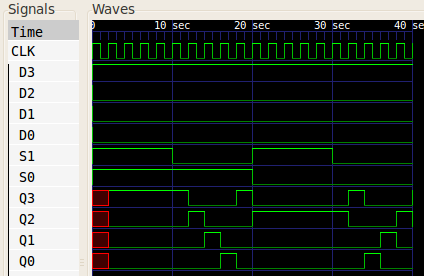
Below you can see the waveforms produced when the register was given some test inputs (load four times, shift right four times, do nothing four times, and shift left four times).
References
Mano, M. Morris, and Kime, Charles R. Logic and Computer Design Fundamentals. 2nd Edition. Prentice Hall, 2000.