Hardwired Nonprogrammable Control Unit Design Example (Greatest Common Divisor)
The following is an example of an algorithmic state machine (ASM) being used to design a hardwired nonprogrammable control unit.
Problem Description
We want to calculate the greatest common divisor (gcd) of two positive integers. The mathematical specification of the gcd function is shown below:
gcd(a,a) = a
gcd(a,b) = gcd(a-b, b)    if a>b,
gcd(a,b) = gcd(a, b-a)    otherwise.
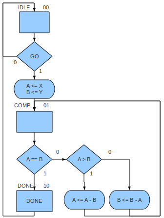
Algorithmic State Machine
The first step is converting the mathematical specification into an ASM.
The following is just such an ASM.
It comprises three states (IDLE, COMP, and DONE),
two registers (A and B),
three inputs (X, Y, and GO),
and two outputs (DONE and either A or B — let's choose A).
If the initial state is IDLE and the arguments of the gcd function are X and Y, then gcd(X,Y)
will eventually be loaded into A.
The input GO starts the whole process, and the output DONE is pulsed (0 to 1) when
A contains the result.
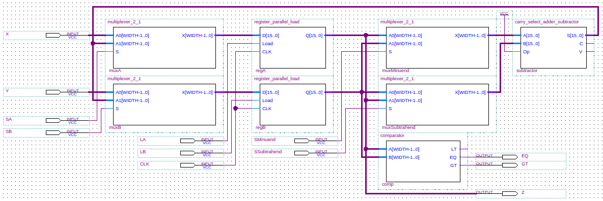
Datapath
Analysing the ASM we see that any destination of a register transfer will need to be a register,
so we need registers A and B.
The RTL operations performed give us the
combinational logic circuits needed.
In this case we need a subtractor.
From analysing the decisions in the ASM we also need a comparator which can signal "equal" and "greater than".
A 16-bit wide datapath derived from the ASM is shown in schematic form below (the WIDTH parameter used in some blocks
should be 16). The output Z is the result of the calculation.
State Table
Using the information from the ASM and outputs from the datapath (EQ and GT),
we can build the state table shown below.
The output DONE is a Moore output so it can be specified here.
As we have three states, we will need two bits to represent these (22=4). State 11 is unused.
| State | Input | State | Output | ||||
|---|---|---|---|---|---|---|---|
| Current | GO | EQ | GT |
Next | DONE |
||
0 | 0 |
0 | X | X |
0 | 0 |
0 |
0 | 0 |
1 | X | X |
0 | 1 |
0 |
0 | 1 |
X | 0 | 0 |
0 | 1 |
0 |
0 | 1 |
X | X | 1 |
0 | 1 |
0 |
0 | 1 |
X | 1 | X |
1 | 0 |
0 |
1 | 0 |
X | X | X |
0 | 0 |
1 |
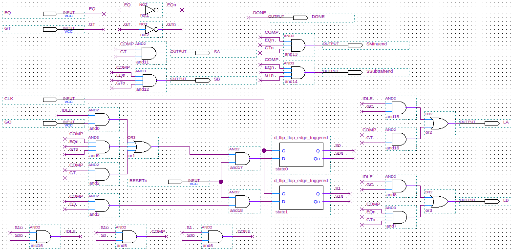
Mealy Outputs
The outputs that control the datapath are Mealy outputs.
A simpler way to express their logic is to decode the binary state code into signals, one for each state.
It makes most sense to give these signals the state names: IDLE, COMP, and DONE.
If we didn't decode like this then each output would use far more gates.
Looking at the datapath we see that the control unit will have to generate signals which will be input to
the two registers (regA and regB) as load signals (LA and LB),
and the four multiplexers (muxA, muxB,
muxMinuend and muxSubtrahend) will need
selection inputs (SA, SB, SMinuend, and SSubtrahend).
The table below shows how these signals are generated.
The contents of the conditions column is expressed in Verilog syntax.
| Datapath Subunit | Signal | Conditions |
|---|---|---|
regA |
LA |
(IDLE & GO) | (COMP & GT) |
regB |
LB |
(IDLE & GO) | (COMP & ~EQ & ~GT) |
muxA |
SA |
COMP & GT |
muxB |
SB |
COMP & ~EQ & ~GT |
muxMinuend |
SMinuend |
COMP & ~EQ & ~GT |
muxSubtrahend |
SSubtrahend |
COMP & ~EQ & ~GT |
The logic from the table can be combined with two D flip-flops to represent state, and
with logic for setting the state to IDLE when an input signal (RESETn) is low.
The resulting schematic, given below, shows that there is much scope for optimisation as many signals are equivalent.
Top-level
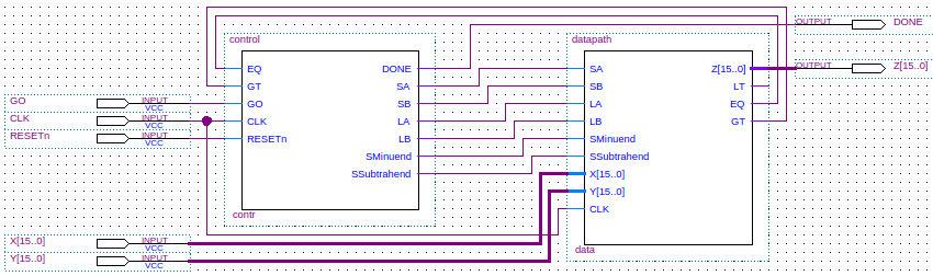
Now we can fit the control unit and datapath together. At the highest level of abstraction, the design looks like this:
Implementation
The full Verilog code for the implementation of the design is shown below.
module gcd(Z, DONE, X, Y, GO, CLK, RESETn);
   output [15:0] Z;
   output 	 DONE;
   input [15:0]  X;
   input [15:0]  Y;
   input 	 GO;
   input 	 CLK;
   input 	 RESETn;

   datapath data(Z, LT, EQ, GT, SA, SB, LA, LB, SMinuend, SSubtrahend, X, Y, CLK);
   control contr(DONE, SA, SB, LA, LB, SMinuend, SSubtrahend, EQ, GT, GO, CLK, RESETn);
endmodule // gcd

module control(DONE, SA, SB, LA, LB, SMinuend, SSubtrahend, EQ, GT, GO, CLK, RESETn);
   output DONE;
   output SA;
   output SB;
   output LA;
   output LB;
   output SMinuend;
   output SSubtrahend;
   input  EQ;
   input  GT;
   input  GO;
   input  CLK;
   input  RESETn;

   wire   IDLE;
   wire   COMP;
   wire   DONE;
   wire   EQn;
   wire   GTn;

   wire   w1, w2, w3, w4, w5, w6, w7, w8, w9;

   not(EQn, EQ);
   not(GTn, GT);

   // States and their transitions.
   d_flip_flop_edge_triggered state0(S0, S0n, CLK, Next0);
   d_flip_flop_edge_triggered state1(S1, S1n, CLK, Next1);

   // Decode the states into signals.
   and(IDLE, S1n, S0n);
   and(COMP, S1n, S0);
   and(DONE, S1, S0n);

   // Logic to give us the next state.
   and(w1, IDLE, GO);
   and(w2, COMP, EQn, GTn);
   and(w3, COMP, GT);
   or(w4, w1, w2, w3);
   and(Next0, RESETn, w4);

   and(w5, COMP, EQ);
   and(Next1, RESETn, w5);


   // The control signals to the datapath - Mealy outputs.
   // These could be optimised to save space, e.g. SMinuend = SSubtrahend = SB
   and(SA, COMP, GT);
   and(SB, COMP, EQn, GTn);
   and(SMinuend, COMP, EQn, GTn);
   and(SSubtrahend, COMP, EQn, GTn);

   and(w6, IDLE, GO);
   and(w7, COMP, GT);
   or(LA, w6, w7);

   and(w8, IDLE, GO);
   and(w9, COMP, EQn, GTn);
   or(LB, w8, w9);

endmodule // control

module datapath(Z, LT, EQ, GT, SA, SB, LA, LB, SMinuend, SSubtrahend, X, Y, CLK);
   output [15:0] Z;
   output 	      LT;
   output 	      EQ;
   output 	      GT;
   input  	      SA;
   input  	      SB;
   input  	      LA;
   input  	      LB;
   input  	      SMinuend;
   input  	      SSubtrahend;
   input [15:0]  X;
   input [15:0]  Y;
   input 	      CLK;

   wire [15:0] 	      A;
   wire [15:0] 	      B;
   wire [15:0] 	      DA;
   wire [15:0] 	      DB;
   wire [15:0] 	      Minuend;
   wire [15:0] 	      Subtrahend;
   wire [15:0] 	      Difference;   // Difference = Minuend - Subtrahend
   wire 	      Borrow;
   wire 	      Overflow;

   assign Z=A;
   multiplexer_2_1 muxA1(DA, X, Difference, SA);
   multiplexer_2_1 muxB1(DB, Y, Difference, SB);
   register_parallel_load regA(A, DA, LA, CLK);
   register_parallel_load regB(B, DB, LB, CLK);
   multiplexer_2_1 muxMinuend(Minuend, A, B, SMinuend);
   multiplexer_2_1 muxSubtrahend(Subtrahend, B, A, SSubtrahend);
   comparator comp(LT, EQ, GT, A, B);
   carry_select_adder_subtractor subtractor(Difference, Borrow, Overflow, Minuend, Subtrahend, 1'b1);
endmodule // datapath


module comparator(LT, EQ, GT, A, B);
   parameter WIDTH=16;     // How many bits wide are the lines
   output LT;
   output EQ;
   output GT;
   input [WIDTH-1:0] A;
   input [WIDTH-1:0] B;

   assign LT = (A < B) ? 1 : 0;
   assign EQ = (A == B) ? 1 : 0;
   assign GT = ~LT & ~EQ;
endmodule // comparator

module register_parallel_load(Q, D, Load, CLK);
   output [15:0] Q;
   input [15:0]  D;
   input 	 Load;
   input 	 CLK;

   wire 	 Loadn;
   wire 	 w1, w2, w3, w4, w5, w6, w7, w8, w9, w10, w11, w12;           // Connecting wires.
   wire 	 w13, w14, w15, w16, w17, w18, w19, w20, w21, w22, w23, w24;  // Connecting wires.
   wire 	 w25, w26, w27, w28, w29, w30, w31, w32, w33, w34, w35, w36;  // Connecting wires.
   wire 	 w37, w38, w39, w40, w41, w42, w43, w44, w45, w46, w47, w48;  // Connecting wires.
   wire [15:0] 	 Qn;   // Unused.

   not(Loadn, Load);

   and(w1, Q[0], Loadn);
   and(w2, D[0], Load);
   or(w3, w2, w1);

   and(w4, Q[1], Loadn);
   and(w5, D[1], Load);
   or(w6, w5, w4);

   and(w7, Q[2], Loadn);
   and(w8, D[2], Load);
   or(w9, w8, w7);

   and(w10, Q[3], Loadn);
   and(w11, D[3], Load);
   or(w12, w11, w10);

   and(w13, Q[4], Loadn);
   and(w14, D[4], Load);
   or(w15, w14, w13);

   and(w16, Q[5], Loadn);
   and(w17, D[5], Load);
   or(w18, w17, w16);

   and(w19, Q[6], Loadn);
   and(w20, D[6], Load);
   or(w21, w20, w19);

   and(w22, Q[7], Loadn);
   and(w23, D[7], Load);
   or(w24, w23, w22);

   and(w25, Q[8], Loadn);
   and(w26, D[8], Load);
   or(w27, w26, w25);

   and(w28, Q[9], Loadn);
   and(w29, D[9], Load);
   or(w30, w29, w28);

   and(w31, Q[10], Loadn);
   and(w32, D[10], Load);
   or(w33, w32, w31);

   and(w34, Q[11], Loadn);
   and(w35, D[11], Load);
   or(w36, w35, w34);

   and(w37, Q[12], Loadn);
   and(w38, D[12], Load);
   or(w39, w38, w37);

   and(w40, Q[13], Loadn);
   and(w41, D[13], Load);
   or(w42, w41, w40);

   and(w43, Q[14], Loadn);
   and(w44, D[14], Load);
   or(w45, w44, w43);

   and(w46, Q[15], Loadn);
   and(w47, D[15], Load);
   or(w48, w47, w46);

   d_flip_flop_edge_triggered dff0(Q[0], Qn[0], CLK, w3);
   d_flip_flop_edge_triggered dff1(Q[1], Qn[1], CLK, w6);
   d_flip_flop_edge_triggered dff2(Q[2], Qn[2], CLK, w9);
   d_flip_flop_edge_triggered dff3(Q[3], Qn[3], CLK, w12);
   d_flip_flop_edge_triggered dff4(Q[4], Qn[4], CLK, w15);
   d_flip_flop_edge_triggered dff5(Q[5], Qn[5], CLK, w18);
   d_flip_flop_edge_triggered dff6(Q[6], Qn[6], CLK, w21);
   d_flip_flop_edge_triggered dff7(Q[7], Qn[7], CLK, w24);
   d_flip_flop_edge_triggered dff8(Q[8], Qn[8], CLK, w27);
   d_flip_flop_edge_triggered dff9(Q[9], Qn[9], CLK, w30);
   d_flip_flop_edge_triggered dff10(Q[10], Qn[10], CLK, w33);
   d_flip_flop_edge_triggered dff11(Q[11], Qn[11], CLK, w36);
   d_flip_flop_edge_triggered dff12(Q[12], Qn[12], CLK, w39);
   d_flip_flop_edge_triggered dff13(Q[13], Qn[13], CLK, w42);
   d_flip_flop_edge_triggered dff14(Q[14], Qn[14], CLK, w45);
   d_flip_flop_edge_triggered dff15(Q[15], Qn[15], CLK, w48);

endmodule // register_parallel_load

module d_flip_flop_edge_triggered(Q, Qn, C, D);
   output Q;
   output Qn;
   input  C;
   input  D;

   wire   Cn;   // Control input to the D latch.
   wire   Cnn;  // Control input to the SR latch.
   wire   DQ;   // Output from the D latch, inputs to the gated SR latch.
   wire   DQn;  // Output from the D latch, inputs to the gated SR latch.

   not(Cn, C);
   not(Cnn, Cn);
   d_latch dl(DQ, DQn, Cn, D);
   sr_latch_gated sr(Q, Qn, Cnn, DQ, DQn);
endmodule // d_flip_flop_edge_triggered

module d_latch(Q, Qn, G, D);
   output Q;
   output Qn;
   input  G;
   input  D;

   wire   Dn;
   wire   D1;
   wire   Dn1;

   not(Dn, D);
   and(D1, G, D);
   and(Dn1, G, Dn);
   nor(Qn, D1, Q);
   nor(Q, Dn1, Qn);
endmodule // d_latch

module sr_latch_gated(Q, Qn, G, S, R);
   output Q;
   output Qn;
   input  G;
   input  S;
   input  R;

   wire   S1;
   wire   R1;

   and(S1, G, S);
   and(R1, G, R);
   nor(Qn, S1, Q);
   nor(Q, R1, Qn);
endmodule // sr_latch_gated

module carry_select_adder_subtractor(S, C, V, A, B, Op);
   output [15:0] S;   // The 16-bit sum/difference.
   output 	 C;   // The 1-bit carry/borrow status.
   output 	 V;   // The 1-bit overflow status.
   input [15:0]  A;   // The 16-bit augend/minuend.
   input [15:0]  B;   // The 16-bit addend/subtrahend.
   input 	 Op;  // The operation: 0 => Add, 1=>Subtract.

   wire 	 C15; // The carry out bit of adder/subtractor, used to generate final carry/borrrow.
   wire [15:0] 	 Bx;

   // Looking at the truth table for not we see that
   // B xor 0 = B, and
   // B xor 1 = not(B).
   // So, if Op==1 means we are subtracting, then
   // adding A and B xor Op alog with setting the first
   // carry bit to Op, will give us a result of
   // A+B when Op==0, and A+not(B)+1 when Op==1.
   // Note that not(B)+1 is the 2's complement of B, so
   // this gives us subtraction.
   xor(Bx[0], B[0], Op);
   xor(Bx[1], B[1], Op);
   xor(Bx[2], B[2], Op);
   xor(Bx[3], B[3], Op);
   xor(Bx[4], B[4], Op);
   xor(Bx[5], B[5], Op);
   xor(Bx[6], B[6], Op);
   xor(Bx[7], B[7], Op);
   xor(Bx[8], B[8], Op);
   xor(Bx[9], B[9], Op);
   xor(Bx[10], B[10], Op);
   xor(Bx[11], B[11], Op);
   xor(Bx[12], B[12], Op);
   xor(Bx[13], B[13], Op);
   xor(Bx[14], B[14], Op);
   xor(Bx[15], B[15], Op);
   xor(C, C15, Op);            // Carry = C15 for addition, Carry = not(C15) for subtraction.
   carry_select_adder csa(S, C15, V, A, Bx, Op);
endmodule // carry_select_adder_subtractor

module carry_select_adder(S, C, V, A, B, Cin);
   output [15:0] S;   // The 16-bit sum.
   output 	 C;   // The 1-bit carry.
   output 	 V;   // The 1-bit overflow status.
   input [15:0]  A;   // The 16-bit augend.
   input [15:0]  B;   // The 16-bit addend.
   input 	 Cin; // The initial carry in.

   wire [3:0] 	S1_0;   // Nibble 1 sum output with carry input 0.
   wire [3:0] 	S1_1;   // Nibble 1 sum output with carry input 1.
   wire [3:0] 	S2_0;   // Nibble 2 sum output with carry input 0.
   wire [3:0] 	S2_1;   // Nibble 2 sum output with carry input 1.
   wire [3:0] 	S3_0;   // Nibble 3 sum output with carry input 0.
   wire [3:0] 	S3_1;   // Nibble 3 sum output with carry input 1.
   wire 	C1_0;   // Nibble 1 carry output with carry input 0.
   wire 	C1_1;   // Nibble 1 carry output with carry input 1.
   wire 	C2_0;   // Nibble 2 carry output with carry input 0.
   wire 	C2_1;   // Nibble 2 carry output with carry input 1.
   wire 	C3_0;   // Nibble 3 carry output with carry input 0.
   wire 	C3_1;   // Nibble 3 carry output with carry input 1.
   wire 	C0;     // Nibble 0 carry output used to select multiplexer output.
   wire 	C1;     // Nibble 1 carry output used to select multiplexer output.
   wire 	C2;     // Nibble 2 carry output used to select multiplexer output.
   wire         V0;     // Nibble 0 overflow output.
   wire 	V1_0;   // Nibble 1 overflow output with carry input 0.
   wire 	V1_1;   // Nibble 1 overflow output with carry input 1.
   wire 	V2_0;   // Nibble 2 overflow output with carry input 0.
   wire 	V2_1;   // Nibble 2 overflow output with carry input 1.
   wire 	V3_0;   // Nibble 3 overflow output with carry input 0.
   wire 	V3_1;   // Nibble 3 overflow output with carry input 1.

   ripple_carry_adder rc_nibble_0(S[3:0], C0, V0, A[3:0], B[3:0], Cin);          // Calculate S nibble 0.
   ripple_carry_adder rc_nibble_1_carry_0(S1_0, C1_0, V1_0, A[7:4], B[7:4], 0);      // Calculate S nibble 1 with carry input 0.
   ripple_carry_adder rc_nibble_1_carry_1(S1_1, C1_1, V1_1, A[7:4], B[7:4], 1);      // Calculate S nibble 1 with carry input 1.
   ripple_carry_adder rc_nibble_2_carry_0(S2_0, C2_0, V2_0, A[11:8], B[11:8], 0);    // Calculate S nibble 2 with carry input 0.
   ripple_carry_adder rc_nibble_2_carry_1(S2_1, C2_1, V2_1, A[11:8], B[11:8], 1);    // Calculate S nibble 2 with carry input 1.
   ripple_carry_adder rc_nibble_3_carry_0(S3_0, C3_0, V3_0, A[15:12], B[15:12], 0);  // Calculate S nibble 3 with carry input 0.
   ripple_carry_adder rc_nibble_3_carry_1(S3_1, C3_1, V3_1, A[15:12], B[15:12], 1);  // Calculate S nibble 3 with carry input 1.

   multiplexer_2_1 #(1) muxc1(C1, C1_0, C1_1, C0); // C0 selects the carry output for nibble 1.
   multiplexer_2_1 #(1) muxc2(C2, C2_0, C2_1, C1); // C1 selects the carry output for nibble 2.
   multiplexer_2_1 #(1) muxc(C, C3_0, C3_1, C2);   // C2 selects the carry output for nibble 3 which is the global carry output.
   multiplexer_2_1 #(1) muxv(V, V3_0, V3_1, C2);   // C2 selects the overflow output for nibble 3 which is the global overflow output.

   multiplexer_2_1 #(4) muxs1(S[7:4], S1_0, S1_1, C0);    // C0 selects the result for nibble 1.
   multiplexer_2_1 #(4) muxs2(S[11:8], S2_0, S2_1, C1);   // C1 selects the result for nibble 2.
   multiplexer_2_1 #(4) muxs3(S[15:12], S3_0, S3_1, C2);  // C2 selects the result for nibble 3.
endmodule // carry_select_adder

module ripple_carry_adder(S, C, V, A, B, Cin);
   output [3:0] S;   // The 4-bit sum.
   output 	C;   // The 1-bit carry.
   output       V;   // The 1-bit overflow status.
   input [3:0] 	A;   // The 4-bit augend.
   input [3:0] 	B;   // The 4-bit addend.
   input 	Cin; // The carry input.

   wire 	C0; // The carry out bit of fa0, the carry in bit of fa1.
   wire 	C1; // The carry out bit of fa1, the carry in bit of fa2.
   wire 	C2; // The carry out bit of fa2, the carry in bit of fa3.

   full_adder fa0(S[0], C0, A[0], B[0], Cin);    // Least significant bit.
   full_adder fa1(S[1], C1, A[1], B[1], C0);
   full_adder fa2(S[2], C2, A[2], B[2], C1);
   full_adder fa3(S[3], C, A[3], B[3], C2);    // Most significant bit.
   xor(V, C, C2);  // Overflow
endmodule // ripple_carry_adder

module full_adder(S, Cout, A, B, Cin);
   output S;
   output Cout;
   input  A;
   input  B;
   input  Cin;

   wire   w1;
   wire   w2;
   wire   w3;
   wire   w4;

   xor(w1, A, B);
   xor(S, Cin, w1);
   and(w2, A, B);
   and(w3, A, Cin);
   and(w4, B, Cin);
   or(Cout, w2, w3, w4);
endmodule // full_adder

module multiplexer_2_1(X, A0, A1, S);
   parameter WIDTH=16;     // How many bits wide are the lines

   output [WIDTH-1:0] X;   // The output line

   input [WIDTH-1:0]  A1;  // Input line with id 1'b1
   input [WIDTH-1:0]  A0;  // Input line with id 1'b0
   input 	      S;  // Selection bit

   assign X = (S == 1'b0) ? A0 : A1;
endmodule // multiplexer_2_1
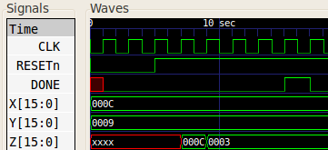
A simulation of the above code gave the following waveform which shows that gcd(12,9) = 3.